
2024 Inductees
Hariklia “Lili” Deligianni, Ph.D.
Founder, Sense4me, Inc.
Former Research Scientist
IBM Thomas J. Watson Research Center
167 U.S. Patents
Dr. Hariklia “Lili” Deligianni is the founder of Sense4me, Inc., a start-up company in digital health with the vision to empower individuals with addiction issues to manage their condition successfully. In 2018, Dr. Deligianni retired from IBM following a distinguished career spanning three decades at the Thomas J. Watson Research Center. She also currently serves as an Adjunct Professor at Columbia University’s Electrochemical Energy Center.
Dr. Deligianni’s pioneering research has had widespread impact across disciplines and industries. Most recently, her work is aimed at developing novel products such as a DNA sequencing electrochemical device; and a toolbox of nanomaterials and nanodevices for brain and peripheral neural stimulation, recordings, and neurochemistry measurements; as well as innovations in wearables, biosensors, bioelectronics, neural interfaces, and artificial intelligence, with applications in neural and mental health.
While at IBM, Dr. Deligianni played a leading role in the successful introduction of electrochemical technology in semiconductor chips, including the co-invention of the copper electrodeposition process for on-chip interconnects, which revolutionized the performance of computer chips and led to world-wide commercialization of electronic components for the semiconductor and telecommunications industries. Dr. Deligianni has also made significant contributions to renewable energy with the development and scale-up of thin film solar cells.
Dr. Deligianni is a member of the National Academy of Engineering. In 2004, she was part of the IBM team honored with the U.S. National Medal of Technology and Innovation for their groundbreaking technologies. Additionally, she is a Fellow of the Electrochemical Society and was the first female recipient of the Vittorio de Nora Award of the Electrochemical Society. She was also recognized with the E.V. Murphree award of the American Chemical Society. She is also a senior member of IEEE and AIChE, and a member of ACS and AAAS. Dr. Deligianni’s innovations have been recognized by Inventor of the Year Award of the New York Intellectual Property Law Association, and she has received multiple IBM Corporate Awards. Dr. Deligianni received her Ph.D. in Chemical Engineering from the University of Illinois Urbana-Champaign.
A Mention About Invention
3 Questions for the Inventor
Q1. Of your patents/inventions, which one is your favorite and why?
U.S. Patent 6,709,562B1 is my favorite. The development of electroplated copper interconnects for the computer industry is a story of perseverance and an underdog winning the race.
The transition from aluminum to copper interconnects in semiconductor technology marked a significant milestone in the industry. Copper interconnects, first introduced by IBM in 1997, revolutionized the fabrication of integrated circuits (ICs) by offering superior electrical properties and enabling the development of faster and more scalable microprocessors. Before the introduction of copper interconnects, aluminum was the standard material used for wiring in ICs. However, as transistor sizes continued to shrink, the limitations of aluminum became apparent. Aluminum interconnects suffered from higher electrical resistance and susceptibility to electromigration, which limited the performance and reliability of computer chips. Copper was identified as a superior alternative to aluminum due to its lower electrical resistance and better electromigration resistance. Copper interconnects reduce propagation delays and power consumption, leading to better overall performance of computer chips.
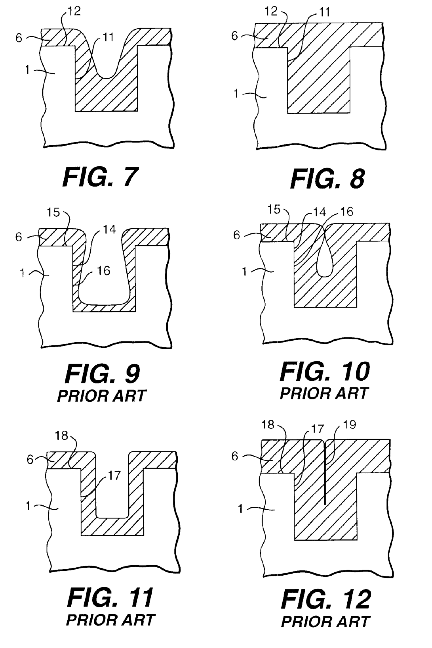
For this major technological implementation, we had to overcome significant challenges in selecting the copper deposition method. Most engineers and scientists were familiar with traditional deposition methods like chemical vapor deposition and sputtering. Many of our colleagues at IBM and throughout the semiconductor industry believed that electroplating was a “dirty” process and entirely incompatible with silicon processing. However, as shown in Figures 7 and 8 of the patent, the deposits produced by electrodeposition were far superior to those produced by sputtering and chemical vapor deposition (as illustrated in Figures 8, 9, 10, and 11 of the prior art). Chemical vapor deposition and sputtering were initially considered but proved inadequate for yielding void-free, seamless, and low-resistivity copper deposits.
Finally, in 1997, IBM and the entire semiconductor industry settled on the underdog, electroplating—a process that uses an electrical charge to draw copper ions from a liquid and deposit copper on the silicon wafer. However, despite the use of electroplated copper in manufacturing since 1997, the patent was filed two years later, in 1999, and it took six years to be allowed and issued! The attorneys and patent examiners alike could not initially understand and appreciate the novelty of the method. To get it through the USPTO, IBM had to argue the case in patent court, where I represented all the inventors. I had to explain that electroplated copper offered three main advantages: it produced bottom-up, void-free filling of features, lower resistivity, and higher reliability of copper due to the chemistry of the electroplating solution.
Q2. What inspired you to become an inventor/innovator?
First and foremost, I have amazing mentors, such as the late Luby Romankiw, who revolutionized magnetic disk storage and enabled an increase in storage density by over seven orders of magnitude. My academic advisor from UIUC, Richard Alkire, taught me by example how to think when tackling a complex problem, and many female colleagues acted as role models and encouraged me to be unstoppable.
My mentors inspired me to do my best work and helped me develop several guiding principles:
- Get a good, basic education. It is worth the sacrifice no matter what the adversities of life are, and be prepared to learn new things for the rest of your life.
- Have an open, curious mind. Recognize when the problem isn’t what others say the problem is.
- Build your intuition, and then trust it. Go the extra mile and persevere. If you feel your idea is right, then be confident in yourself and never give up.
- Put your heart, mind, and soul into what you are doing. Let others see your enthusiasm for what you do.
- Do not take no for an answer… No means not right now. Keep your optimism and keep going.
- Later, once you have proven feasibility, let go of your ideas so they can bloom in the minds of others. Then, take pride when others enable your ideas to succeed beyond what you could have imagined.
Equally important in the innovation process is to surround yourself with a team of colleagues that challenge you to excel. Technology innovation is certainly a team sport! We always worked with a multidisciplinary and geographically diverse group of colleagues who brought their own backgrounds, education, and experiences into the innovation process and greatly contributed to the team’s success. As a result, we have always innovated as a group, and the resulting 260+ patents reflect a diverse group of co-inventors.
Q3. What is your process when developing new inventions/innovations?
The process is about re-inventing yourself every few years! I have always learned to challenge myself and transitioned from innovations in the electronics industry to developing and scaling up thin film solar cells and renewable energy sources, to neural engineering, biosensors, and brain-computer interfaces, and to applying artificial intelligence (AI) in the medical and wellness domain. I have leveraged my extensive background in electrochemical engineering and the computer industry to apply my skills in new domains.
For example, I have created tools and sensors that can help understand and treat diseases of the nervous system, indicating a full-circle change as I apply my engineering expertise to biomedical challenges.
My motivation for these changes is driven by my passion for tackling complex problems, a trait I cultivated during my Ph.D. at the University of Illinois in Urbana-Champaign and then during my time at IBM. I thrive on changing directions every few years, which has allowed me to explore various scientific fields and contribute to innovative solutions in each. My transition from microelectronics to renewable energy, to neural engineering and artificial intelligence, is marked by my desire to apply my technical skills to new challenges in biomedical research, reflecting my adaptability to learn new domains and my lifelong commitment to scientific innovation.